Dalam pengadaan elektronik, istilah PCB sering dipakai terlalu longgar. Banyak tim meminta penawaran PCB padahal yang dibutuhkan sebenarnya adalah board terakit, firmware, kabel, dan uji fungsi.
PCB berarti printed circuit board, yaitu board kosong. Ketika komponen sudah dipasang dan disolder, produknya menjadi PCBA. SMT adalah proses perakitan, bukan nama produknya.
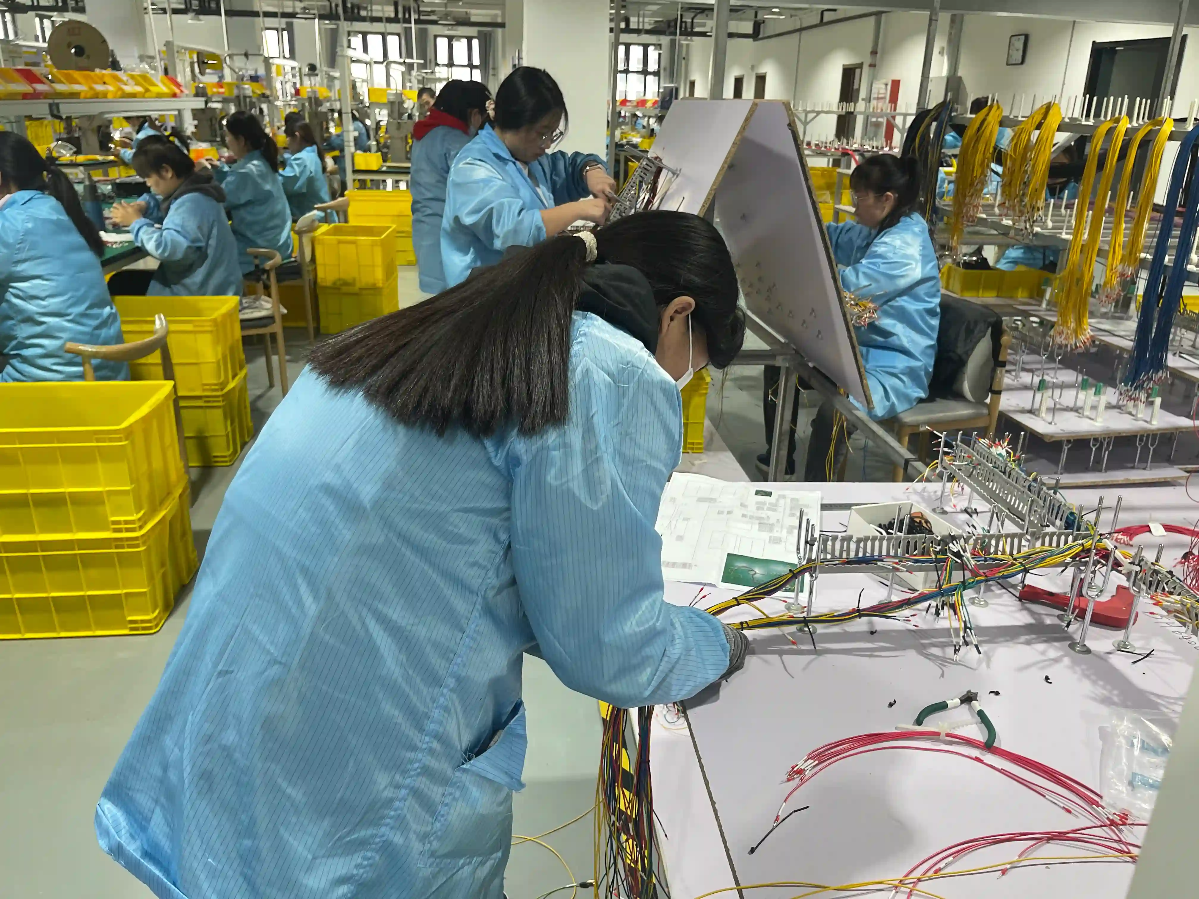
If your product includes both boards and cable assemblies, define the interconnect scope early. That means connector series, mating orientation, current load, wire gauge, strain relief, environmental exposure, and test coverage. Clear scope at RFQ stage prevents re-quotes, NPI delays, and first-article failures caused by mismatched board-to-wire interfaces.
1. Apa arti PCB yang sebenarnya
PCB stands for printed circuit board. In B2B manufacturing language, that means the fabricated board before component loading: substrate, copper pattern, drilled holes, plated vias, solder mask, silkscreen legend, and surface finish. It does not automatically include components, soldering, firmware flashing, conformal coating, depaneling, box build, or cable integration.
This distinction matters because bare-board suppliers, PCB assembly suppliers, and full system integrators quote different scopes, tooling assumptions, minimum order quantities, and quality records. If the RFQ says "PCB" but the attached files imply a full assembled module, the first quote is often wrong before engineering review even starts.
PCB
Bare fabricated board only: laminate, copper, holes, mask, legend, finish.
PCBA
Assembled board: PCB plus components, soldering, inspection, and often test.
SMT
Surface mount technology: one process used during assembly, not the product itself.
2. PCB vs PCBA vs SMT
Buyers should use PCB when requesting fabrication only, PCBA when requesting components and assembly, and SMT when discussing the placement process, line capability, package compatibility, or stencil-and-reflow controls. Mixing the terms creates avoidable confusion around whether pricing includes procurement, AOI, X-ray, ICT, FCT, programming, or burn-in.
A quick rule works well in sourcing meetings: if the board can leave the factory with no components mounted, it is a PCB; if it leaves with components soldered, it is PCBA; if you are talking about chip placement, paste printing, reflow profile, tombstoning, or 0201/BGA capability, you are talking about SMT.
| Term | What It Means | Usually Included | Common RFQ Files |
|---|---|---|---|
| PCB | Bare fabricated board | Material, copper, drill, finish, electrical test | Gerber/ODB++, drill, stackup, fab notes |
| PCBA | Assembled circuit board | PCB + components + assembly + inspection/test | Gerber/ODB++, BOM, XY, assembly drawing, test notes |
| SMT | Surface mount assembly process | Stencil, placement, reflow, AOI, process control | Package data, panel info, DFM notes, process limits |
3. Board terbuat dari apa
Most commercial boards start with FR-4 epoxy-glass laminate, then add copper foil, drilled and plated vias, solder mask, silkscreen, and a final finish such as ENIG or HASL. Higher-performance programs may move to polyimide for flex, aluminum-core for thermal management, or low-loss RF materials such as Rogers for controlled high-frequency performance.
When buyers ask what a circuit board is made of, the practical answer is not just “fiberglass and copper.” The real specification includes dielectric system, Tg value, copper weight, layer count, impedance targets, via structure, finish type, thickness tolerance, UL flame rating, and any compliance requirement such as RoHS, REACH, or IPC class level.
| Board Element | Why It Matters to Buyers |
|---|---|
| Base material | Cost, thermal behavior, flex performance, signal integrity |
| Copper weight | Current carrying capacity, trace width, heat rise |
| Layer count | Routing density, EMI control, stackup complexity, cost |
| Surface finish | Shelf life, solderability, fine-pitch performance, cost |
| Via structure | Density, reliability, HDI capability, lead time |
| Testing and class | Yield expectations, documentation, acceptance criteria |
4. Apa yang harus dikirim bersama RFQ
For bare PCB pricing, send Gerber or ODB++ data, drill data, stackup, finished thickness, copper weight, finish, solder-mask color, panel preference, quantity, and compliance targets. For PCBA, add a clean BOM, pick-and-place data, assembly drawing, approved substitutions policy, programming needs, and inspection or functional-test requirements.
If the product also includes wire harnesses or cable assemblies, send the connector part numbers, mating orientation, harness drawing, wire list, current and voltage, environment, bend constraints, labeling, and end-of-line test plan. Buyers who submit board files without the interconnect package usually trigger re-quotation after DFM review because the board-to-wire scope was incomplete.
Minimum RFQ Package
Gerber or ODB++ files and drill data
BOM, approved AVL/alternates, and assembly drawing if PCBA is required
Quantity by build stage: prototype, EVT/DVT/PVT, and production
Environment, compliance target, and test/documentation requirements
Connector and harness drawings for any board-to-wire integration
5. Apa yang mendorong biaya, lead time, dan ruang lingkup pengujian
Board cost moves fastest when layer count increases, impedance control is added, via structures become more complex, copper gets heavier, or the finish shifts from a low-cost option to ENIG, hard gold, or specialized RF material. Lead time stretches further when buyers combine hard-to-source ICs, tight mechanical tolerances, custom test fixtures, firmware loading, conformal coating, or full box-build integration.
Testing scope must match product risk. A simple bare PCB may only need electrical test, while an assembled control module may need AOI, X-ray for BGA or QFN, ICT or flying probe, functional test, programming verification, and cable continuity checks. The more clearly buyers define risk, reliability target, and field environment, the easier it is for suppliers to quote the right process without padding price or schedule.
| Driver | Impact on Price | Impact on Lead Time |
|---|---|---|
| Higher layer count or HDI | Higher fabrication and yield risk | Longer engineering and fabrication cycle |
| Special material or finish | Material premium | Longer procurement window |
| PCBA with constrained components | BOM volatility and buying risk | Longer sourcing cycle |
| Functional test + cable integration | Fixture and labor cost | Longer NPI and validation phase |
For mixed board-and-harness projects, ask suppliers to confirm ownership of each deliverable: bare PCB, component procurement, PCBA, firmware loading, cable assembly, box build, and final test. Ambiguity at this step is a common cause of cost creep.
6. Pertanyaan umum
Apakah PCB berarti board sudah terpasang komponen?
Tidak. PCB biasanya hanya berarti board kosong. Setelah komponen dipasang dan disolder, istilah yang benar adalah PCBA.
Apakah SMT sama dengan PCBA?
Tidak persis. SMT adalah proses manufaktur yang digunakan saat perakitan, sedangkan PCBA adalah board rakitan akhir.
Apa yang harus saya kirim jika produk saya mencakup PCB dan wire harness?
Kirim data fabrikasi board, BOM, gambar assembly, nomor part konektor, gambar harness, kuantitas per tahap, lingkungan penggunaan, target lead time, dan target kepatuhan.